
































Samsung Pledges $108 Billion to Build HBM, OLED and Battery Hubs in South Korea
Samsung Group will invest 144 trillion won, about $108 billion, in South Korea's Chungcheong region, building new hubs for HBM chip packaging, OLED displays, AI server substrates and batteries, with the first plants due to start operating from 2028.
Samsung Pledges $108 Billion to Build HBM, OLED and Battery Hubs in South Korea
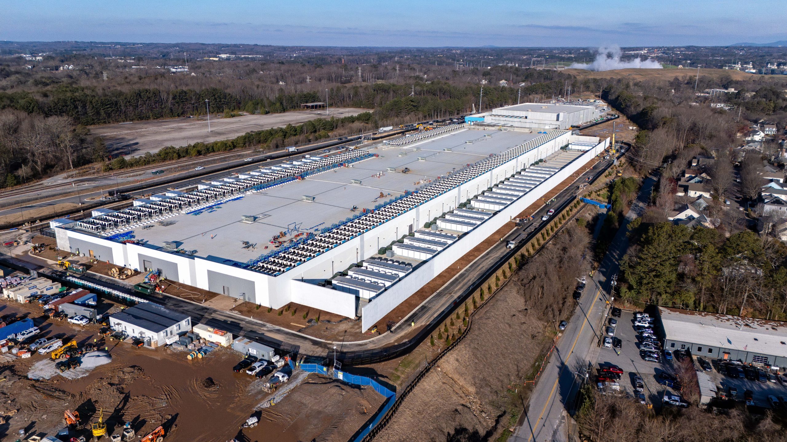
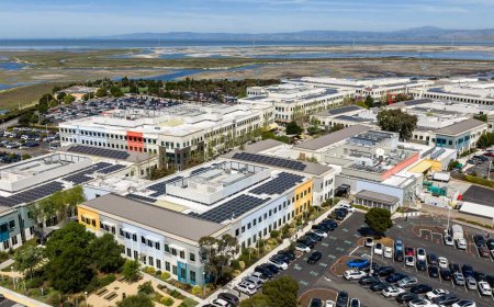
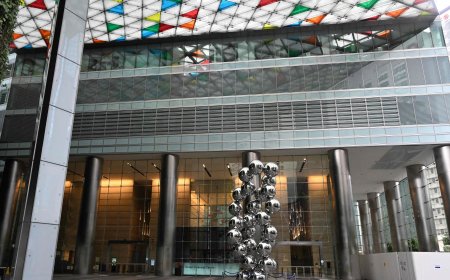
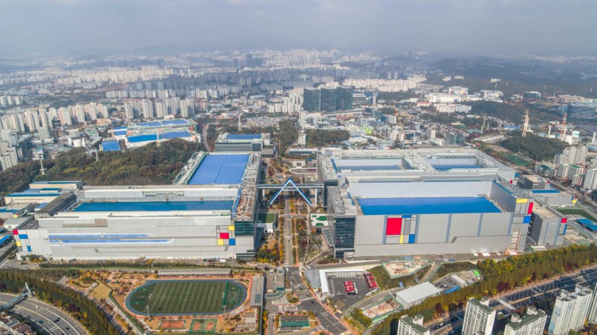
Photo: Samsung's semiconductor manufacturing complex in Hwaseong, South Korea.
Samsung Group is committing 144 trillion won — roughly $108 billion — to turn South Korea's Chungcheong region into a manufacturing heartland for the artificial intelligence era. The plan, unveiled at a groundbreaking ceremony on November 12, spans high-bandwidth memory (HBM) packaging, OLED displays, AI server components and batteries, with the first of the new plants due to start operating in 2028.
South Korean President Lee Jae-myung attended the ceremony at Samsung Electronics' Onyang campus in Asan, alongside Samsung Executive Chairman Lee Jae-yong, as the group raised its regional commitment from the 140 trillion won announced in July.
A 144 trillion won plan across four affiliates
The investment is split between four Samsung affiliates. Samsung Electronics will put in 60 trillion won, Samsung Display 67 trillion won, Samsung Electro-Mechanics 8 trillion won and Samsung SDI 9 trillion won. Together they will build advanced semiconductor packaging facilities, OLED panel production lines, package substrate plants for AI servers and battery manufacturing sites across Asan, Cheonan and Sejong.
The ceremony marked the groundbreaking of three projects at once: Samsung Electronics' advanced packaging fab in Onyang, Samsung Display's production line in Asan and Samsung Electro-Mechanics' AI server substrate plant in Sejong.
Onyang Line 5: the HBM packaging hub
The centrepiece for Samsung Electronics is a fifth production line at its Onyang campus, dedicated to advanced packaging for next-generation HBM — the high-bandwidth memory that sits beside AI accelerators in data centres and has become one of the most sought-after components in the AI boom.
Foundation work on Onyang Line 5 is already under way, and operations are scheduled to begin in June 2028, about a year earlier than originally planned. The facility will hold 9,400 pyeong of cleanroom space across three floors. Samsung Electronics will invest 46 trillion won in the Onyang site in phases, including 6 trillion won for construction and 40 trillion won for advanced equipment, and it also plans to expand and modernise HBM-related facilities at its existing Cheonan site.
"This site, which previously focused on simple assembly and testing of conventional semiconductors, will transform into a cutting-edge HBM hub at the heart of AI semiconductors," Chairman Lee Jae-yong said in his welcoming remarks.
Jun Young-hyun, vice chairman and head of Samsung Electronics' Device Solutions division, said the company would work with suppliers to strengthen the semiconductor production base connecting Onyang and Cheonan and develop the Chungcheong region into the world's leading hub for advanced packaging.
Displays, substrates and batteries
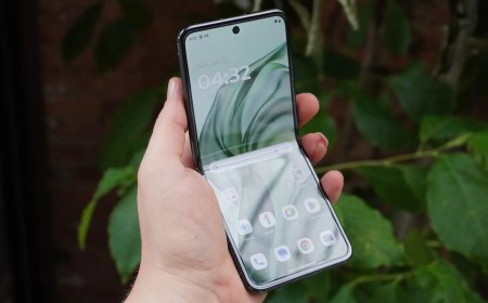
Samsung Display is taking the largest share of the commitment. Its 67 trillion won will fund OLED production in Asan and Cheonan, led by the A7 line in Asan, which broke ground in October. The line will span 170,000 pyeong across three floors, with 5.9 trillion won earmarked to produce OLED panels for foldable smartphones, laptops and tablets, targeting mass production in the second half of 2029. Foldable phones are a market Samsung already leads — the company held about two-thirds of global foldable shipments in the third quarter, according to analysts, as reported in our Samsung foldable market share story.
Samsung Electro-Mechanics will invest 8 trillion won at its Sejong site to expand capacity for AI semiconductor package substrates, the boards that connect advanced chips inside AI servers. It will spend 4.3 trillion won on a new four-storey factory that broke ground last month and covers 30,000 pyeong, with mass production scheduled for September 2028. The company also plans to secure additional nearby land to expand the business further.
Samsung SDI will invest 9 trillion won at its Cheonan site, which is being developed as a "mother factory" for next-generation battery technologies. Construction of the Cheonan battery mother factory was completed in July last year, equipment operations began that November, and additional equipment is currently being installed.
Suppliers and jobs
Samsung's suppliers are moving in step with the group. Kim Young-jae, chairman of Daeduck Electronics and of Samsung Electronics' supplier council, said at the ceremony that 194 domestic semiconductor materials, components and equipment companies plan to invest about 18.1 trillion won by 2030. Of those, 66 companies are investing or preparing to invest 4.4 trillion won in the Chungcheong region, and the investments are expected to create around 23,000 jobs.
President Lee said the central and local governments would work as one team to handle permits and key infrastructure, including electricity and water, so the investment plans proceed without disruption. South Chungcheong Province and Asan City had already shortened the permitting process to about one-third of its usual duration, helping construction start sooner.
At a joint public-private review meeting after the ceremony, Lee said six of the eight companies in the Chungcheong investment initiative had begun investing, and that 112 companies plan to invest a further 23.6 trillion won in sectors including semiconductors and biotechnology, on top of a previously announced 392 trillion won regional investment plan.
"What matters is action, not words, and execution, not promises," the president said. Chairman Lee Jae-yong added that Samsung would pursue mega projects in the Honam and Yeongnam regions as well, "to create an irreplaceable Korean success story."
Why it matters
The announcement lands as demand for HBM and AI infrastructure keeps climbing, and as Samsung works to close the gap with rivals in the memory market. Packaging — the step that stacks and connects HBM chips to AI processors — has become a bottleneck in its own right, which is why the Onyang investment is aimed squarely at it rather than at wafer production.
The scale and the speed also matter. Raising the commitment by 4 trillion won in four months, bringing the Onyang start forward by a year and breaking ground on three plants at once all point to a group trying to move faster than its competitors. For South Korea, the plan spreads high-value manufacturing beyond the Seoul area and ties the Chungcheong region's fortunes more tightly to the global AI supply chain.
Sources
What's Your Reaction?
 Like
0
 Dislike
0
 Love
0
 Funny
0
 Angry
0
 Sad
0
 Wow
0